The semiconductor industry is a cornerstone of modern technology, powering everything from smartphones to supercomputers. Behind the scenes, a crucial component of semiconductor manufacturing is the use of test wafers.
These unassuming discs of silicon play a pivotal role in ensuring the quality and reliability of semiconductor devices. In this blog post, we will delve into the world of test wafer solutions, exploring their significance, challenges, and best practices.
Introduction to Test Wafer Solutions in the Semiconductor Industry
Test wafers are miniature versions of the silicon wafers used to manufacture integrated circuits (ICs) and other semiconductor devices. They are employed primarily for testing and characterization purposes.
Unlike production wafers, which yield thousands of chips, they typically contain a limited number of devices. These devices mimic the actual ICs in terms of design and functionality, making them ideal for evaluating the manufacturing process and the performance of the final products.
The Role of Test Wafers in Semiconductor Manufacturing
In the production of semiconductors, sample wafers, often referred to as cmp wafers, serve two crucial purposes. They play a pivotal role in supporting process development and optimization first.
Engineers rely on these CMP wafers to ensure that the production slabs consistently yield high-quality chips by fine-tuning manufacturing procedures. Moreover, CMP wafers are instrumental in uncovering flaws early in the manufacturing cycle, making them indispensable for quality control.
This early diagnosis not only minimizes waste but also enhances the overall dependability of the final product.
Key Challenges in Development and Testing
Development and testing present several formidable challenges. Firstly, replicating the exact conditions of production wafers on a smaller scale is a complex task, as even minor deviations can lead to inaccurate results.
Secondly, ensuring the reproducibility of defects for reliability testing can be intricate, requiring meticulous control of variables. Material selection is critical, as different materials have distinct properties that must closely match those of production wafers to yield meaningful insights.
Moreover, designing test structures and devices that mimic production counterparts demands precision. Lastly, maintaining consistency and repeatability throughout the fabrication process is essential for reliable testing outcomes.
Overcoming these challenges requires expertise, advanced technology, and a commitment to adhering to best practices in development and testing.
Importance of Material Selection

Material selection is a critical consideration when crafting them. Silicon is the most common choice due to its similarity to production wafers, but other materials like gallium arsenide may be used for specialized applications.
The material’s properties, such as crystal orientation and doping levels, must closely match those of production wafers to yield meaningful results.
Design Considerations
The design is another crucial factor. Devices on test wafers should mimic those on production wafers as closely as possible, including their size, spacing, and electrical characteristics.
Additionally, test structures, like sensors and test circuits, are integrated to facilitate performance evaluation and defect detection.
Best Practices for Fabrication Processes
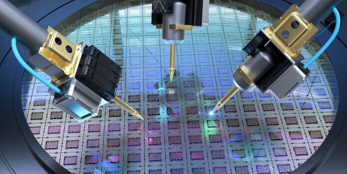
Implementing best practices in test wafer fabrication processes is essential for achieving reliable and accurate results. Cleanroom environments must maintain strict cleanliness and contamination control measures to prevent defects.
Precise lithography and etching processes are crucial to creating test structures that faithfully mimic production devices. Rigorous inspection and metrology at each fabrication stage ensure that the wafers meet desired specifications. Automation and handling systems minimize contamination risks and human errors during production.
Consistency and repeatability are paramount, demanding tight process control and adherence to standardized procedures.
By following these best practices, semiconductor manufacturers can produce high-quality test wafers that serve as invaluable tools for process development, quality control, and innovation, ultimately leading to improved product reliability and cost-effectiveness.
Quality Control Measures in Production
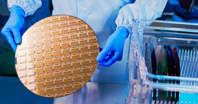
Quality control is integral to production. Statistical process control (SPC) techniques are often employed to monitor the manufacturing process and identify variations. Advanced imaging and inspection tools are used to detect defects, while automated handling systems minimize contamination risks during production.
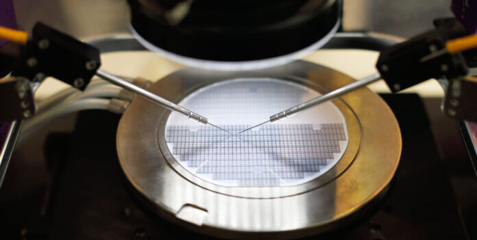
Testing Methodologies and Techniques
Testing methodologies vary depending on the objectives. Electrical testing assesses the functionality of devices, while thermal testing evaluates their heat dissipation capabilities. Reliability tests, such as accelerated aging, are crucial to predict the lifespan of semiconductor devices.
Case Studies Showcasing Successful Solutions
Let’s explore a couple of case studies that exemplify the impact of effective solutions:
Case Study 1: Intel’s Advanced Lithography Optimization
Challenge: Intel, a global leader in semiconductor manufacturing, faced a significant challenge in optimizing their advanced lithography process for the production of cutting-edge microprocessors. Ensuring the quality and yield of these complex chips demanded a comprehensive approach.
Solution: Intel employed meticulously designed ones that featured test structures representing various device types and feature sizes. They enabled engineers to identify process variations and defects early in the development cycle, providing valuable insights.
Outcome: The utilization led to a substantial reduction in production costs and a notable increase in the yield of defect-free chips. By fine-tuning its lithography process based on insights gained from them, Intel maintained its position at the forefront of semiconductor technology.
Case Study 2: ABC MEMS Technologies’ Reliability Enhancement
Challenge: ABC MEMS Technologies, a leader in microelectromechanical systems (MEMS) manufacturing, faced the challenge of ensuring the reliability of their MEMS devices in critical applications like automotive sensors.
Solution: ABC MEMS Technologies employed specialized ones that incorporated sensors for real-time data collection during testing. This allowed for a comprehensive reliability assessment.
Outcome: By leveraging them in this manner, ABC MEMS Technologies achieved enhanced product reliability, leading to increased customer satisfaction and confidence in their MEMS devices. Their innovative approach strengthened their market position and facilitated broader adoption of MEMS technology in various industries.
Future Trends and Innovations in Technology
The semiconductor industry is in a perpetual state of evolution, and they are no exception. As technology advances, we can expect to see innovations such as 3D test wafers that mimic complex three-dimensional device structures, and the integration of artificial intelligence and machine learning for more efficient defect detection and process optimization.
Conclusion and the Impact on Semiconductor Success
In conclusion, they are the unsung heroes of the semiconductor industry, playing a pivotal role in ensuring the quality, reliability, and cost-effectiveness of semiconductor devices. Through careful material selection, design, fabrication, and testing, manufacturers can harness the power to unlock success in a highly competitive industry.
As technology continues to advance, the importance will only grow, enabling semiconductor companies to push the boundaries of innovation while maintaining the highest standards of quality. By embracing best practices and staying at the forefront of this technology, these companies can continue to drive progress and shape the future of the digital age.


